EinEinfach
Well-known member
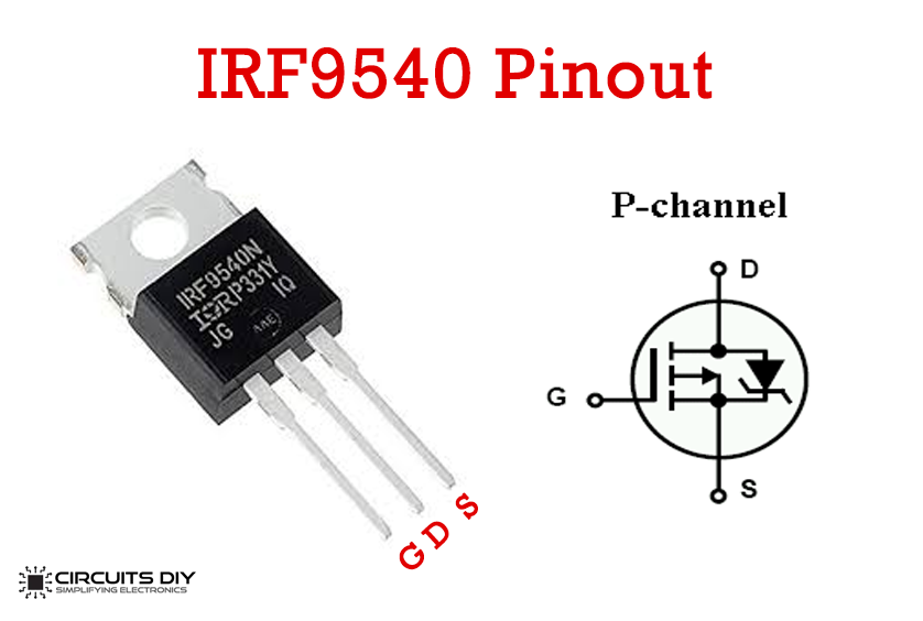
Can you share your Drain Source Gate pinout, I can't find it datasheet
Or wait a moment... it is a p-chanel MOSFET then is that ok Drain + and Source - should be diode voltage. But why it works as expected if I change drain and source wiring... I'm out of ideas...But if I measure with multimeter Drain + and Source -, I see diode voltage, what is ok is if I would measure Source + and Drain -.
Yes is enough (1.2mm should be also ok)The hole is currently 1.1mm, is 1.3mm enough?
I think current version isn't trash, with small modifications it is still useableI don't want to throw any more circuit boards in the Trash.
I'm still working on it, I don't know, when I will be done. Just let me know if you want place the order, if I'm done with my design, then we can order both of themIf you have your PCB ready, should I also order it, saves shipping costs?
 github.com
Yes, if you twist the pins, but it's not so nice, it's supposed to be proper.I think current version isn't trash, with small modifications it is still useable
")
I don't remember, but I think i don't use SB1240 but smaller one to fit in the hole.One more thing, the holes for D3 and D5 are to small I have to drill out it to get mount SB1240

Wired everything together, seems to running, but no time to perform further tests. Maybe on friday.The circuit board would be ready to order, unless you find something else
OkWired everything together, seems to running, but no time to perform further tests. Maybe on friday.
That can i change.What about marks scl and sda, in my opinion it should be also changed, no one from us has INA with marked sda and scl pinout.
Can you confirm that it works like this?And last but not least, what about that:
New wiring of INA
I recently saw a solution where you can set the address of the INAS via jumpers on the PCB without soldering the Inas. I thought it was a good idea, but of course I didn't save it.Also it would be helpful to put both I2C together as option, maybe two jumpers what connects SDA1 with SDA0 and SCL0 with SCL1. If someone (like me) is using only one I2C then he/she have to connect jumpers if not just leave it without