Landrumower Protected&Cool MOD

RD123

Active member
Clipboard01.jpg
Clipboard02.jpg
Clipboard03.jpg
Landrumower Protected&Cool MOD
!!!!!!!!!!!!!!!!!!!!!!!!!!!!!!!!!!!!!!!!!!!!!!!!!!!!!!!!!!!!!!!!!!!
Experimental version ! Not yet tested. As Is. Can not work.
!!!!!!!!!!!!!!!!!!!!!!!!!!!!!!!!!!!!!!!!!!!!!!!!!!!!!!!!!!!!!!!!!!!

Totally optional version of the board. The main goal is to isolate the electronics from power/motor circuits overvoltages. And cool it. Experimental. Not as cheap and simple, but with few extra features.

Changelog:
V. 1.0 initial release.


Links:
Version with TPS12110:
Version: 1.00 links removed (bugged)

Version 1.01 (will be uploaded only after physical testing in few weeks)

Version with ITS428L2
Version 1.00 links removed (bugged)

Version 1.01 (will be uploaded only after physical testing in few weeks)


-Main board.
Some pull up/pull down resistors/rc filter need to be put onto the board, please refer to original Landrumower scheme/findings info.

To do it, there are left some smd 0805 resistor footprints with 3 pads. Resistor can be not soldered (no-pull up/down), or soldered in 2 position. Either pull-up or pull-down configuration as needed, on that footprint can be selected.

Please keep in mind to calculate the total power that can be delivered by Raspberry pins and not use too strong pull up/down resistors for all lines altogether.


Also do not use together opposite options in example:

Software pull-down

pinBumperX = Pin(18, Pin.IN, Pin.PULL_DOWN)

Resistor Pull-up configuration.
Conflict. Not ok.

Software pull-down
Resistor pull-down

Sometimes should be OK.(their combined resistance is reduced,higher current draw, can introduce slow rise times or oscillations).

Preferably software pull should be switched off.

Software pull-down
Resistor not put.

OK. But software pull up/down could be sometimes weak.

Software Pull-down not selected
Resistor Pull-down.
Ok.

GPIO Electrical Specifications, Raspberry Pi Input and Output Pin Voltage and Current Capability
 
Last edited:
-Power board.
Please refer to all information from other boards iterations, posted on the forum.

Selectable:

-overvoltage
-undervoltage => hardware protection of Li-Po 7s for overdischarge (BMS should be installed anyway on lipo pack.)
-2 stage overcurrent (selectable level)
-overtemperature
-ideal diode
-N-MOSFET switch controlled by 3,3V-20V
-protected Mosfet driver.
-Inrush current control.
Charging rate of capacitors can be adjusted.

BLDC motors needs a lot of capacitors, large amount of capacitors creating inrush problem during switching on:

Lets take a look at the voltage drop during BLDC work:


Based on/rework of:


To do:

-add format/annotation to schemes to be more readable to human.

-optional cheap bldc motor driver pcb with built-in selectable overcurrent/overvoltages logic, then simplify boards.

-version with smd MOSFET (DPAK)
 
Why Tps12110?

Features
• AEC-Q100 qualified
–40°C to +125°C ambient
• Functional Safety-Capable
• 3.5V to 40V input range (45V absolute maximum)
• Output reverse polarity protection down to –30V
• Integrated 12V charge pump with 100µA capacity
• Low 0.9µA shutdown current (EN/UVLO = Low)
• Strong pullup (3.7A) and pulldown (4A) gate driver
• Drives external back-to-back N-channel MOSFETs
• Variant with integrated pre-charge switch driver
(TPS12111-Q1) to drive capacitive loads
• Two-level adjustable overcurrent protection
(IWRN, ISCP) with adjustable response time
(TMR) and fault flag output (FLT_I)
• Fast short-circuit protection: 1.2µs (TPS12111-Q1, TPS12112-Q1), 4µs (TPS12110-Q1)
• Accurate analog current monitor output (IMON):
±2% at 30mV (VSNS)
• Accurate, adjustable undervoltage lockout (UVLO) and overvoltage protection (OV): < ±2%
• Remote overtemperature sensing (DIODE) and protection with fault flag output (FLT_T)
• Pin-to-pin compatible with TPS4811-Q1

Needed parameters of resistors/capacitors should be calculated using attached calculator in XLS file.

Please refer to IC datasheets/reference notes.
-possibility to use large current.

Cooled:

-swapped IRF9540 Mosfet from 0,2 Ohm (24v/10A=20W) to 6 mOhm N-channel Mosfet ((24v/10A=0.5W)

-Introducing ideal diode controller, eliminating Schottky diodes.

P=0.7V×10A
P=7 W
2 diodes eliminated in line:
2x7W =14W

Replaced by 0,5W Mosfet+ LM5050 (2x0,5W MOSFET in TPS12110)

=20W+14W-1,5W=32,5W of power not lost to heat=cool PCB
-large power tracks/return ground path
-separating power/digital/gnd1 grounds
-Some isolated signal/I2C line chips, should in theory also act as a I2C signal repeater (in the middle of the line).

-Changed shunt resistor on INA226 to 0.004 ohm ERJMS4SF4M0U or equivalent. That change will allow to measure up to 20,48 A (also less heat is generated on that resistor 0,004 vs 0,01 ohm).

Multiplier then need to be updated in firmware. If needed to go back to 8,19A limit as it was before, then use ERJMS4HF10MU 0,01 shunt.

 
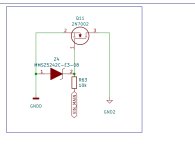
-added optional safety braking resistor circuit for BLDC driver especially for MOW motor.

Why?

Bldc motor act as a GENERATOR when rotating, generated energy need to be dissipated somewhere. If not, it increasing voltage in circuit, electrocuting all electronics.

Mistral.ai
deepai.org/chat

Example worst case scenario:

How many energy will have disc (mow) with diameter 40cm. Mass 1000g rotated with 3000 rpm. Slowed down to 0 rpm in 10s. That disc is connected to generator. How much will rise the temperature of resistor with weight 50g from 20 Celsius. 2 ohm resistor is made from 60% ceramic, 35% aluminum, 5% kanthal?
(...)
The energy dissipated as heat in the 2-ohm resistor is 986.96 J

So, the temperature of the resistor will rise to approximately 44.67 °C.

Generator is given 986.96 J energy to convert to electricity. What will be the final voltage stored in 470uf capacitor?
(...)
So, the final voltage stored in the 470 μF capacitor will be approximately 2049.37 volts.
(Voltage without dumping energy to heat).
(...)
986.96 J energy dumped in to-220 Mosfet not heatsinked over the time of 10s. What will be the Mosfet temperature?
(...)
Estimated temperature rise: ~7402°C (theoretical)

Practical outcome: The MOSFET will likely vaporizing or burning out.

And with heatsink?

If the heatsink is efficient and Rθ_is about 10 °C/W, the MOSFET will reach roughly 987°C

Not possible to survive energy dump without power resistor or dumping energy back to battery.

Some of the features can be replaced/dropped as per need.

Tps12110 can be replaced by tps48xx chip (higher voltage version) or replaced by 2x ITS428L2

All 3.3v, 5v power supply ics, can be swapped by simplier, cheaper version of circuit/ic.

Ideal diode ICs can be swapped with normal diodes, but then it need to be mounted on heatsink.

Other Isolators (2 x cheaper) with less lines (ISO6741F), can be used with minor change to the scheme (with failsafe option = low), i just reusing some old IC stocks. DIY.

Jumpers/potentiometer/multiple value of the resistors/capacitor selectable options could be removed, there are just put on PCB for experimental version.

Isolators can be dropped and replaced by voltage translators. Then there is no need to use isolated power supply but = limited protection.

In case of problems with powering Raspberry Pi 5 through GPIO, then Raspberry 5 need to be powered through USB-C port, read more info on post in forum.

The best approach (because of complexity) is to order smt stencil during PCB ordering, order parts separately and assembly in home. Keeped minimum 0805 smt parts size, for easy assembly.

Size of the board <100 mm for cost/manufacturing considerations.

Thermal reliefs are removed (for better electrical connection=higher A). I will assembly PCB on hot plate. If using other methods, please consider readding it. Also hand solder footprints are not selected, if using soldering iron, it is better to replace it normal -> hand solder, and check position of footprints on the PCB, they are slightly bigger.


Or use 0,2mm soldering tin wire and soldering iron:


Use only nylon/plastic screws/cable ties to mount PCBs.

Do not accidentally mix GNDs.

If using cable shielding, connect shield to GND only on one side of PCB.

-Parameters can be calculated using attached calculator and value of the resistor can be inputed on empty 0805 smd space. There is also possibility for set the parameters using potentiometers/resistors + jumper (optional).

Jumpers are for isolation of the potentiometer during ohm setting/disconnecting. Resistors can be swapped for potentiometer footprint, but I don't know how potentiometer will behave during vibration when mowing. Not yet tested.


There is possibility to put some digital potentiometer like AD5243/AD5248 etc.


But the safest cheapest solution is just preset values with regular resistors/capacitors that can be calculated using attached xls calculator.

-Changed layout for Increasing tracks width.

-some safety diodes/mosfet on scheme are removed.

(charger side)

If You need it back please look at older circuits then DIY.

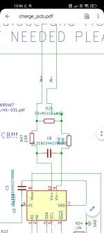
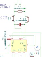
The original charging circuit in ChargePCB v 1.0

Is not optimally designed! Because there is voltage drop on diode + Mosfet

In example:

Vloss = I x Rds

Given:

Rds=0,2 (IRF9540)
I=5A

So, the voltage loss across the MOSFET is 1V.

Diode : 0,6 (even Schottky) + 1V = 1,6 V (!)

So 7s lion will be always charged to 27.8V ~ 70% capacity. Using 29,4V charger.


That diode/mosfet:

-could cause the voltage oscillation with some chargers.

- YouTube
(...)

-could cause problem with BMS. Some models start balancing cells from certain voltages. That is never reached because of diode. (... )

(...) Slow charging causes phase separation. - Martin Z. Bazant | Stanford University | Physics of next generation batteries.(...)*
(...)
The problem with this circuit is that many boards have discharge cut-off circuit(dw01) cant be used as diode will block the discharge completely.
(...)
I did the same test 10 years ago with the same results. A very confused controller.
(...)
If you keep permanently 1.1 Volt across a Ni-MH cell, or 1.8 Volt across a Lead-acid cell, both cell will stay at 25% state of charge without damage.

If you keep 3.8 Volt permanently across a Li-ion cell, it will keep at 25% state of charge, but after a couple of weeks it will be either dead or damaged (increased Ri).*

-When chargers don't cut charging in certain time. With Li-ion battery cells could be damaged:

*Comments in above video.

-With high current chargers voltage drop need to be huge (bigger diode, bigger loss on Mosfet).
(...)
The main circuit diode:

The safety circuit based on Tps1211 have additional Mosfet acting as a ideal diode.

If using Li-on battery, the best solution is to use safe charger that will not burn anything:

- YouTube

Lets take a look at the example charger:


-3-step charge control with current detection

-Universal input voltage

-Wake up and low current start-up of deeply discharged batteries

-Safety indication and protection: Against reverse polarity, short circuit, charging battery packs with the wrong number of cells and safety timer run-out.

Approvals

Medically certified => isolated.

Safety:• UL approved• EN 60601-1 ed. 3.1• Home healthcare EN 60601-1-11• Household safety, EN 60335-1 & -2-29EMC:• EN 60601-1-2 ed. 4

Or other PROTECTED chargers. That all the charging parameters can be adjusted.

And then compare to the quality of other (cheap), no-name power supply from channel:

- YouTube

(...)

"A self-baking, thermal drifting, interference generating, electrocution house burner..."(...)

- YouTube

- YouTube

So what is the choice on the ChargePCB?

-leave it as it was originally =>battery is not fully charged (because of diode+mosfet). Please add missing components on schematics DIY.

-add chip like NCV68261 + n-Mosfet, DIY

-add ITS428L2 + diode, DIY

-skip all the circuits on ChargePCB (except basic one) and leave all the safety circuits on the SAFE CHARGER side (default version).

Charging circuit => is the charger job.

-Xt30 charging input port (will be basic protected by diode and blowing fuse: according to the scheme):


I'm really amazed at your work on the PCB.
Unfortunately, I don't understand all of it either :-)

Is the MainPCB usable now?

I haven't looked at the circuit diagram yet and would match the SMD parts for the BOM file with JLPCB and then order them assembled, i.e. only the SMD components.

Edit: The ISO7762FDW is End of Live
Similar Product: ISO7762FDWR

The circuit diagram of the PowerPCB is not easy to read and understand.
 
Last edited:
I'm really amazed at your work on the PCB.
Unfortunately, I don't understand all of it either :-)

Is the MainPCB usable now?

I haven't looked at the circuit diagram yet and would match the SMD parts for the BOM file with JLPCB and then order them assembled, i.e. only the SMD components.

Edit: The ISO7762FDW is End of Live
Similar Product: ISO7762FDWR

The circuit diagram of the PowerPCB is not easy to read and understand.
(...) Is the MainPCB usable now?(...)
Hard to tell. It is still not tested.
I will answer that question in 2-3 week time.
At the moment it is in production.
IMG_20250709_203825.jpg
Passed DFM. So will be assembled.

I changed mind as how I will assembly PCB.

Mainboard assembly by soldering iron (large enough footprints/pads).

ChargePCB (INA226, all IC, 70% of passive components only basic catalog, 2-3 from extended catalog ). Are put to production for JLCPCB.
Mainly because of how small footprint of INA226 is.
30% passive/SMT I will solder, with soldering iron.

And when I calculated the price of stencil/new soldering paste. Jlcpcb just win.

(...)
The ISO7762FDW is End of Live
Similar Product: ISO7762FDWR

I choosed that IC too.
It need to have similar convention:

ISO7762Fxxxx
F - mean default output (truth table) = low
Mean that in case of power failure the BLDC motor don't start on itself.
Xxxx - next iteration of IC.

Even if it is in the end of life, the IC can be swapped by any IC with default Low failsafe option:

With small change to scheme:

ISO6741F (less lines, cheaper)
Some cheap chinese IC,
ADuM341E0
ADUM141D0BRZ-RL7
4DIR1400H
(...) The circuit diagram of the PowerPCB is not easy to read and understand.(...)

In free time it will be reorganized/ commented.

Some of the parameters of passives can be lowered (like voltage).
 
Screenshot_2025-07-10-11-52-04-609-edit_com.google.android.apps.pdfviewer.jpgTVS diode and capacitors are meant to suppress transient spikes in line input. In example when connecting the battery (sparking) or using the mechanical switch.


R60 current sense resistor (scheme can be configured to check RDSon resistance of Mosfet, but resistor is more precise +/- 2%)
Value of it is calculated using XLS file.

Screenshot_2025-07-10-13-24-36-368-edit_com.google.android.apps.pdfviewer.jpg
 
When settings values for Inrush control it should be used part of XLS:

Calculations for Bootstrapped capacitor, CBST during Inrush current control (dv/dt mode)
Screenshot_2025-07-10-12-11-13-253-edit_com.microsoft.office.excel.jpg

In example for 3000uf 100ms start time the Inrush current is 720ma. For that Cbst=3,3uf C1=330nf. R64=100k, R62=100R.
Screenshot_2025-07-10-12-06-52-741-edit_com.google.android.apps.pdfviewer.jpg
Screenshot_2025-07-10-12-21-30-415-edit_com.google.android.apps.pdfviewer.jpg

The values depends on total capacitance (sum of capacitors on PCB/BLDC drivers), and start time.
In calculator there is also need to put MOSFET gate charge. For IPP057N15NM6AKSA1 the gate charge is 55.
Screenshot_2025-07-10-12-24-44-364-edit_com.google.android.apps.pdfviewer.jpg
When using different Mosfet, charge need to be updated in XLS file.
 
Last edited:
Screenshot_2025-07-10-12-26-27-701-edit_com.google.android.apps.pdfviewer.jpg
Linear voltage converter is to supply 3.3V. It is located after the Tps12110 switch.

Tps12110= off = no voltage from converter

Tps12110= on = 3.3 V signal


It is used to keep Tps12110 On after startup initialisation. Powering voltage isolator/ stop switch.

Linear voltage converter, initialised only when pressing On switch, when Tps12110 will switch up. The second Voltage converter will take over supply.


Schottky diodes D12, D13 are for connecting 2 linear voltage converter together.

ISO7420FED is used to isolate on signal from Raspberry Pi.
 
Last edited:
Additional voltage converters are needed because

Tps12110 as a safety feature need to isolate ground. Ground of Tps12110 are connected using Q11 Mosfet (more info in documentation).

Screenshot_2025-07-10-12-42-06-075-edit_com.google.android.apps.pdfviewer.jpg
TMR capacitors values are calculated using XLS file.
Screenshot_2025-07-10-12-44-30-317-edit_com.google.android.apps.pdfviewer.jpg


In expample:
Level 1 =16,80A

Level 2 =20,16A

That is to set first stage overcurrent. Time after the switch will be OFF. In example 16.80A for Jumper 5 is on (time 1ms), so the current above 16,80A is allowed for set time.

If the time will pass the Tps12110 will be off.

Selecting JP10 with resistor. Will disable timer. When reaching 16,80A in 4us Tps12110 will be off.

Reaching Level 2 =20,16A

Immediate shutdown.

R58 is for setting Level 2. The easiest way is to calculate value and put resistor, skipping potentiometer.
Screenshot_2025-07-10-12-59-21-107-edit_com.google.android.apps.pdfviewer.jpg
 

Attachments

  • Screenshot_2025-07-10-12-42-06-075-edit_com.google.android.apps.pdfviewer.jpg
    Screenshot_2025-07-10-12-42-06-075-edit_com.google.android.apps.pdfviewer.jpg
    82.7 KB · Views: 1
LM5050 circuit is acting as a ideal diode.
Screenshot_2025-07-10-13-01-08-021-edit_com.google.android.apps.pdfviewer.jpg

TVS/ capacitors are for suppressing the transient spikes, during MOSFET ON/OFF transition.
Screenshot_2025-07-10-13-04-41-127-edit_com.google.android.apps.pdfviewer.jpg

Charging circuit is basic protected using only fuse and diode (it protect for reverse connection, more info in previous post).

Screenshot_2025-07-10-13-06-39-891-edit_com.google.android.apps.pdfviewer.jpg
Ina226 is for current/voltage sensing.

The sense resistor is swapped for 4mOhm. The it will allow sensing above 20A. (more info in previous post).


R46, R47, C8 (similar in other INA226 circuits) are for transient protection, act as a filter.


Each INA226 is preset for I2C address. Please check other board iterations for it.
 

Attachments

  • Screenshot_2025-07-10-13-06-24-734_com.google.android.apps.pdfviewer.jpg
    Screenshot_2025-07-10-13-06-24-734_com.google.android.apps.pdfviewer.jpg
    339 KB · Views: 1
  • Screenshot_2025-07-10-13-06-39-891-edit_com.google.android.apps.pdfviewer.jpg
    Screenshot_2025-07-10-13-06-39-891-edit_com.google.android.apps.pdfviewer.jpg
    244.1 KB · Views: 1
  • Screenshot_2025-07-10-13-06-24-734_com.google.android.apps.pdfviewer.jpg
    Screenshot_2025-07-10-13-06-24-734_com.google.android.apps.pdfviewer.jpg
    339 KB · Views: 1
Braking resistor circuit. It will dump excess energy to, power resistor. Scheme explanation in other post in forum.
Screenshot_2025-07-10-13-11-32-381-edit_com.google.android.apps.pdfviewer.jpg

The size of the power resistors for driving motor can be lower value than for MOW motor.

TSR-1-2433...
Screenshot_2025-07-10-13-14-19-814-edit_com.google.android.apps.pdfviewer.jpg

Are for supply of 5V and 3.3 voltage for isolators, BLDC/ high voltage side. They are not isolated.

(They will be dropped in next board iteration.)

ISO1640

Are for isolating I2C signal between Raspberry PI/ high voltage side.
Screenshot_2025-07-10-13-18-23-287-edit_com.google.android.apps.pdfviewer.jpg
 
Screenshot_2025-07-10-13-45-49-386-edit_com.google.android.apps.pdfviewer.jpg
Diode MAIN is for temperature sensing of switching MOSFETS. It will switch off Tps12110 when temperature will be too high.

IMON main is V output that can be used for current measurement. R52 is to set scale. In that example it reach 0-2,7V at 30A.

Screenshot_2025-07-10-14-41-36-305-edit_com.google.android.apps.pdfviewer.jpg

FLT_I_MAIN = overvoltage fault signal
FLT_T_MAIN = temperature fault
IMON_MAIN = current signal /0-2,7V / 30A
 
Last edited:
Tps12110

Can also be replaced with:


Screenshot_2025-07-10-14-09-30-067-edit_com.google.android.apps.pdfviewer.jpg

It have overcurrent set at 17A
With nominal current 7A
If it is too small value load can be split for ie 2 IC.

1IC (drive, +raspberry)
2 IC (mow)

The ChargePCB will be cheaper/smaller with that IC (no sense resistor, MOSFETs already inside the chip, no external passives/resistor /capacitors, so no calculation of values).

Just remove all circuits/resistors/capacitors that belong to Tps12110 and put its428l2.

(INP going to IN in its428l2) the other connection as in its428l2 scheme.


Screenshot_2025-07-10-14-30-21-732-edit_com.google.android.apps.pdfviewer.jpg


DIY.
 
Last edited:
Clipboard04.jpg

!!!!!!!!!!!!!!!!!!!!!!!!!!!!!!!!!!!!!!!!!!!!!!!!!!!!!!!!!!!!!!!!!!!
Experimental version ! Not yet tested. As Is. Can not work.
!!!!!!!!!!!!!!!!!!!!!!!!!!!!!!!!!!!!!!!!!!!!!!!!!!!!!!!!!!!!!!!!!!!

Cheaper/simplier version of ChargePCB with ITS428L2.
7A nominal current.
17A Overcurrent.

If need more current, add 1 more ITS428L2. DIY.
(more info 2 posts above)
 
Last edited:
Experimental Pcbs arrived.
Unfortunately as was mentioned above:

!!!!!!!!!!!!!!!!!!!!!!!!!!!!!!!!!!!!!!!!!!!!!!!!!!!!!!!!!!!!!!!!!!!
Experimental version ! Not yet tested. As Is. Can not work.
!!!!!!!!!!!!!!!!!!!!!!!!!!!!!!!!!!!!!!!!!!!!!!!!!!!!!!!!!!!!!!!!!!!

They are bugged and they need revision of 1.01.

Links to version 1.0 are removed.
Fixed version of 1.01 will be uploaded only after physical assembling/testing in few weeks.
 
Back
Top